FIB Milled Nanochannels
A number of different nanofabrication techniques have been used to fabricate nanofluidic channels, with current state-of-the-art methods able to achieve widths of ca. 10 nm. We developed a focused ion beam (FIB) milling protocol to directly write nanofluidic conduits in fused silica substrates. By milling into the substrate through a thick (> 100 nm) metal film (Figure 1), it was possible to mill features with widths below 5 nm. Using FIB milling, features with gradually varying widths and depths can also be fabricated. One area of study has been the behavior of DNA molecules in three-dimensional nanofunnels (Figure 2). In these structures, a DNA molecule experiences greater confinement as it is electrophoretically driven more deeply into the nanofunnel.
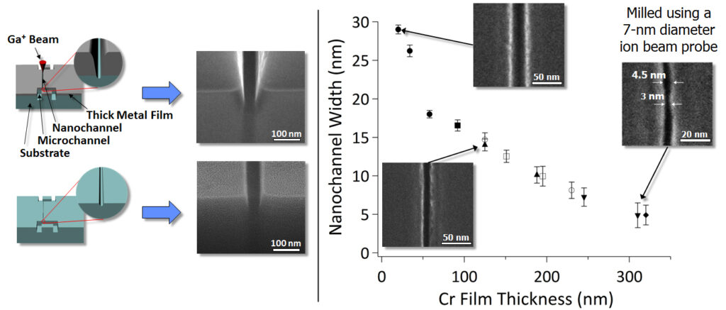
Figure 1. (left) A nanochannel is milled into a substrate through a thick metal film, intersecting previously patterned microfluidic elements. After milling, the metal film is removed using a chemical etchant and the top surface of the channels is sealed by bonding a coverplate to the substrate. The SEM images show cross-sectional views of a 50-nm channel before and after removal of the metal film. (right) The plot shows the dependence of feature width on a chromium film when a 7-nm diameter Ga+ ion beam is linearly rastered over the surface.
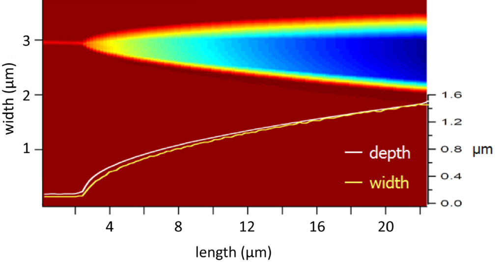
Figure 2. Atomic force microscopy profile of a FIB milled nanofunnel. The spectral gradient indicates the varying depth within the funnel. The identical shape of the width and depth profiles is evident in the inset plots. The depth profile was measured along the nanofunnel’s long axis.
Reference
L. D. Menard and J. M. Ramsey (2011) Fabrication of sub-5 nm nanochannels in insulating substrates using focused ion beam milling. Nano Lett. 11, 512-517.